- 您现在的位置:买卖IC网 > Sheet目录349 > PCA9533DP/01,118 (NXP Semiconductors)IC LED DRIVER RGB 8-TSSOP
NXP Semiconductors
PCA9533
4-bit I 2 C-bus LED dimmer
SDA
SCL
MASTER
TRANSMITTER/
RECEIVER
SLAVE
RECEIVER
SLAVE
TRANSMITTER/
RECEIVER
MASTER
TRANSMITTER
MASTER
TRANSMITTER/
RECEIVER
I 2 C-BUS
MULTIPLEXER
SLAVE
002aaa966
Fig 9.
System con?guration
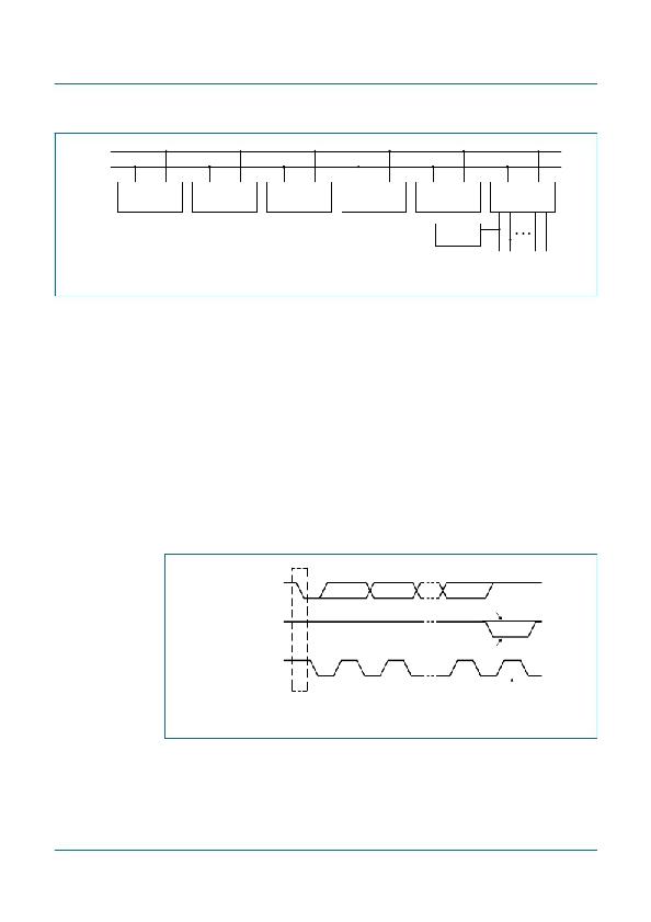
7.3 Acknowledge
The number of data bytes transferred between the START and the STOP conditions from
transmitter to receiver is not limited. Each byte of eight bits is followed by one
acknowledge bit. The acknowledge bit is a HIGH level put on the bus by the transmitter,
whereas the master generates an extra acknowledge related clock pulse.
A slave receiver which is addressed must generate an acknowledge after the reception of
each byte. Also a master must generate an acknowledge after the reception of each byte
that has been clocked out of the slave transmitter. The device that acknowledges has to
pull down the SDA line during the acknowledge clock pulse, so that the SDA line is stable
LOW during the HIGH period of the acknowledge related clock pulse; set-up and hold
times must be taken into account.
A master receiver must signal an end of data to the transmitter by not generating an
acknowledge on the last byte that has been clocked out of the slave. In this event, the
transmitter must leave the data line HIGH to enable the master to generate a STOP
condition.
data output
by transmitter
not acknowledge
data output
by receiver
acknowledge
SCL from master
1
2
8
9
PCA9533_3
S
START
condition
Fig 10. Acknowledgement on the I 2 C-bus
clock pulse for
acknowledgement
002aaa987
? NXP B.V. 2009. All rights reserved.
Product data sheet
Rev. 03 — 27 April 2009
9 of 24
发布紧急采购,3分钟左右您将得到回复。
相关PDF资料
PCA9550DP,118
IC LED DRIVER BLINKER 8-TSSOP
PCA9551BS,118
IC LED DRIVER BLINKER 16-HVQFN
PCA9552D,118
IC LED DRIVER BLINKER 24-SOIC
PCA9553DP/01,118
IC LED DRIVER LINEAR 8-TSSOP
PCA9624PW,118
IC LED DRIVER RGBA 24-TSSOP
PCA9625D/S911,518
IC LED DRIVER RGBA 32-SOIC
PCA9626BS,518
IC LED DRIVER RGBA 48HVQFN
PCA9632DP2,118
IC LED DRIVER RGBA 10-TSSOP
相关代理商/技术参数
PCA9533DP/02
制造商:PHILIPS 制造商全称:NXP Semiconductors 功能描述:4-bit I2C-bus LED dimmer
PCA9533DP/02,118
功能描述:LED照明驱动器 4-BIT I2C-BUS LED DIMMER RoHS:否 制造商:STMicroelectronics 输入电压:11.5 V to 23 V 工作频率: 最大电源电流:1.7 mA 输出电流: 最大工作温度: 安装风格:SMD/SMT 封装 / 箱体:SO-16N
PCA9533DP01
制造商:PHILIPS 制造商全称:NXP Semiconductors 功能描述:4-bit I2C LED dimmer
PCA9533DP02
制造商:PHILIPS 制造商全称:NXP Semiconductors 功能描述:4-bit I2C LED dimmer
PCA9534
制造商:PHILIPS 制造商全称:NXP Semiconductors 功能描述:8-bit I2C and SMBus, low power I/O port with interrupt
PCA9534A
制造商:TI 制造商全称:Texas Instruments 功能描述:REMOTE 8-BIT I2C AND SMBus LOW-POWER I/O EXPANDER WITH INTERRUPT OUTPUT AND CONFIGURATION REGISTERS
PCA9534A_10
制造商:TI 制造商全称:Texas Instruments 功能描述:REMOTE 8-BIT I2C AND SMBus LOW-POWER I/O EXPANDER WITH INTERRUPT OUTPUT AND CONFIGURATION REGISTERS
PCA9534A_101
制造商:TI 制造商全称:Texas Instruments 功能描述:REMOTE 8-BIT I2C AND SMBus LOW-POWER I/O EXPANDER WITH INTERRUPT OUTPUT AND CONFIGURATION REGISTERS
